
Purpose-Built Silicon for Advanced AI.
Eliminating the 1,000W generality tax. Fairview Semiconductor delivers turnkey, air-cooled silicon-to-software platforms — unifying HBM4 memory architecture and MPU compute from individual silicon dies to full data center racks, powering the AI trillion-dollar wave from 2026 to 2036 and beyond.
From Silicon Dies to Turnkey Rack Systems.
Two flagship products. One unified architecture. Infinite AI scale.
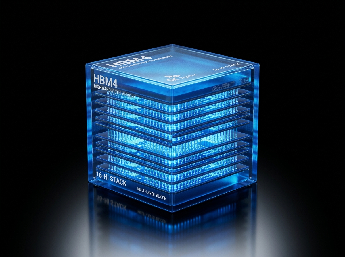
Gallium HBM4 Architecture
Direct die-to-memory attach providing 16.0 TB/s throughput for data-intensive AI models and high-efficiency training clusters. The Gallium Series redefines what memory bandwidth means for next-generation AI infrastructure.
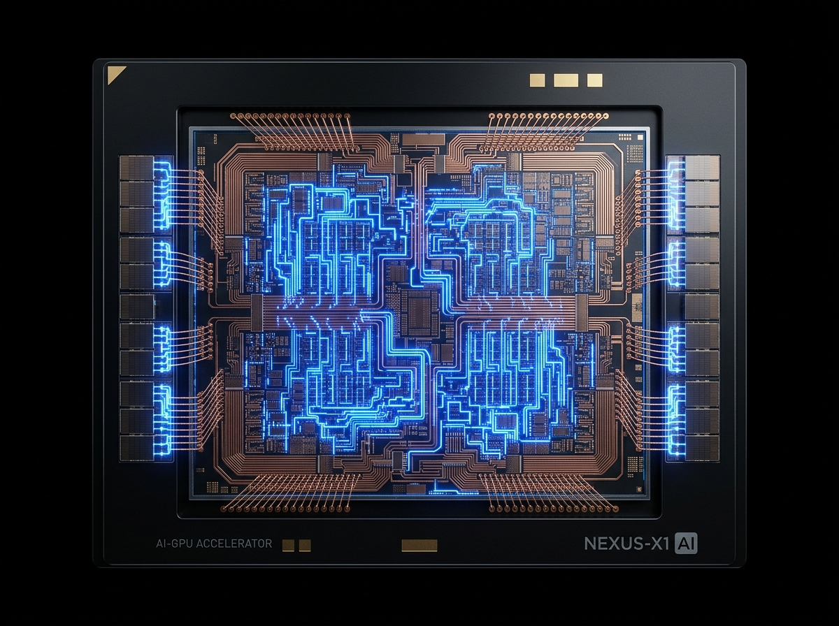
Stallion AI Accelerator
2nm GAAFET (TSMC N2) compute die optimized for tensor execution and high-bandwidth memory access across dense AI infrastructure. The Stallion Series delivers unmatched parallel compute for LLM training, inference, and hyperscale AI workloads.
High-Intensity AI Silicon Without the GPU Overhead
Fairview Semiconductor bridges the gap between inefficient general-purpose GPUs and brittle, unprogrammable ASICs.
Stallion™ MPU
350W Pure Systolic Tensor Engine
Pure systolic tensor engines designed exclusively for deterministic enterprise LLM inference. We strip out the 1000W generality tax of legacy graphics pipelines to deliver 350W air-cooled efficiency.
Gallium™ Fabric
Direct Zero-Copy Topology
Programmable scale-out interconnect delivering direct memory-to-memory zero-copy topology. Eliminates third-party networking bottlenecks to seamlessly scale from a 2U blade to a full Sovereign POD.
Tiered NVM Architecture
Near-Memory Data Access
Advanced tiered memory integration leveraging Non-Volatile Memory (NVM) architectures. Breaks the memory wall by optimizing near-memory data access for massive model parameters.
KV-Cache Subsystem
High-Throughput Persistent Memory
High-throughput persistent storage subsystem engineered specifically for continuous agentic context memory and massive KV-cache retention, ensuring zero-latency recall for BFSI pipelines.
The Scaling Dilemma in Frontier AI
The GPU Silicon Overhead
General-purpose GPUs allocate less than 10% of total die registers to raw matrix compute, wasting massive silicon real estate and power on complex instruction decoding, dynamic warp scheduling, and cache coherence.
The Rigid ASIC Trap
Single-architecture hardwired ASICs risk immediate obsolescence as frontier model topologies shift (e.g., Mixture-of-Experts, State Space Models, hybrid attention), while pure-SRAM approaches lack the memory density required for multi-billion-parameter workloads.
The Fairview Solution
Fairview Semiconductor re-architects compute from the transistor level up—combining maximum math-to-die density with programmable linear algebra primitives and next-generation wide-bus HBM4 integration.
Competitive Architecture Comparison Matrix
Target comparison at product scale (not measured silicon).
| Feature | Legacy GPUs (H100/B200) | Pure-SRAM ASICs (Groq) | Hardwired ASICs | Fairview Semiconductor |
|---|---|---|---|---|
| Math-to-Die Area | Low (~5–10% active math registers) | Moderate (Dominated by SRAM cells) | High (>30% fixed logic) | High (>35% flexible tensor execution) |
| Memory Architecture | Legacy Discrete DRAM | Pure SRAM (~230 MB capacity) | Legacy Standard Memory | 16,384-bit HBM4 Wide-Bus Interface |
| Model Versatility | Universal (High overhead) | Moderate (Kernel compilation bound) | Zero (Hardwired to standard attention) | High (Programmable Matrix ISA) |
| Sparsity Acceleration | Software/Driver mediated | Minimal | None (Fixed dense dot products) | Hardware-Native 2:4 Sparsity Decoding |
| Scalability Bottleneck | Thermal / Power / Schedulers | Massive multi-hundred chip clustering | Algorithmic shifts / Model changes | Balanced Compute-to-Bandwidth Ratio |
1U, 2U & 3U High-Density Blade Servers.
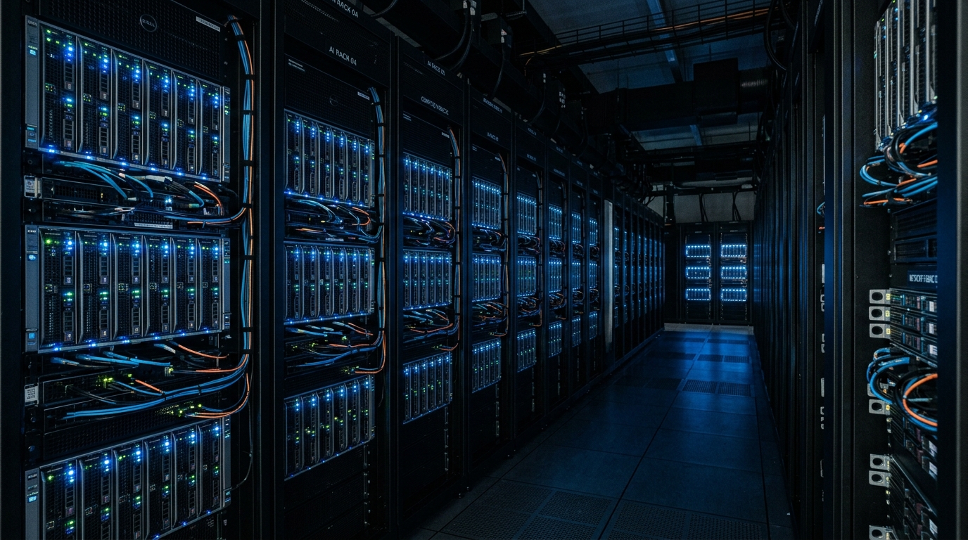
- Compute4x Stallion S80I
- Use CaseHigh-Density Inference & Edge
- CoolingHigh-Static Air
- NetworkDual 800GbE OSFP
- Compute8x Stallion S80I
- Use CaseLLM Training & Hyperscale AI
- CoolingDirect-to-Chip Liquid
- NetworkQuad 800GbE OSFP
- Compute16x Stallion S80I
- Use CaseRack-Scale Supercomputing
- CoolingFull Liquid Immersion
- Network8x 800GbE OSFP
Purpose-Built for Sovereign & Enterprise Infrastructure.
Delivering dedicated, high-efficiency compute platforms tailored for regulated banking, sovereign national security, and high-availability enterprise infrastructure.
Algorithmic Trade Surveillance & Sovereign Core-Banking LLMs
Ultra-low latency, deterministic inference for algorithmic trade surveillance, AML monitoring, and sovereign core-banking LLMs executing directly on-premise without third-party API exposure.
The 3Dx3D Heterogeneous Glass Core Substrate.
Target co-packaged architecture (product family).
Eliminating the Memory Wall.
From single silicon dies to datacenter racks — conventional AI architectures separate compute from memory, creating severe latency bottlenecks. FairView unifies high-throughput Stallion MPU dies directly with Gallium HBM4 memory on a single 2.5D substrate, scaling into turnkey enterprise blade systems for 2027–2028 deployments.
Request Early Access & Technical Datasheets.
Direct engagement for Stallion MPU silicon samples, Gallium HBM4 pinout specs, and official engineering datasheets.